4.4 Multi-Level Caches and Coherence
The computational power of a modern multi-core, superscalar, and SIMD-enabled processor requires a high-throughput memory system. Parallel execution engines require a high volume of instructions and data, but main memory (DRAM) access is orders of magnitude slower than the processor’s clock cycle. This performance gap between the CPU and main memory is known as the “memory wall,” and it represents a significant bottleneck in modern computer architecture.1 To address this gap, CPUs employ a supporting architecture built around a multi-level memory hierarchy and a protocol for maintaining data consistency across multiple cores.
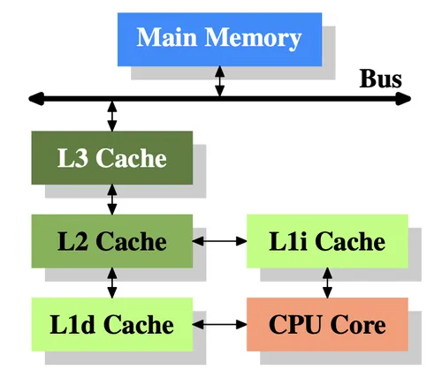
Image Credit: Based on a diagram from “What Every Programmer Should Know About Memory” by Ulrich Drepper.
The Multi-Level Cache Hierarchy
Section titled “The Multi-Level Cache Hierarchy”The primary technique to mitigate the memory wall is the multi-level cache hierarchy, a system of small, fast, on-chip memory (SRAM) that holds copies of frequently used data and instructions from main memory. When the processor needs data, it first checks the fastest, closest level of cache. If the data is present (a “cache hit”), it is delivered to the core in a few clock cycles. If it is not present (a “cache miss”), the processor checks the next, larger and slower level of cache. If the data is not in any cache, the processor accesses main memory.2 Modern CPUs typically feature three levels of cache:
- Level 1 (L1) Cache: This is the smallest and fastest cache, located closest to the processor’s execution units. A typical L1 cache access has a latency of a few clock cycles. To maximize bandwidth and reduce contention, the L1 cache is almost always split into an L1 instruction cache (L1i) and an L1 data cache (L1d). In a multi-core processor, each core has its own private L1 cache.2
- Level 2 (L2) Cache: The L2 cache is larger and slower than the L1 cache. It services L1 misses. If data is not found in L1, the L2 is checked before an access to the L3 or main memory is initiated. In many modern designs, each core has its own private L2 cache, though some architectures have used shared L2 designs.2
- Level 3 (L3) Cache / Last-Level Cache (LLC): The L3 cache is the largest and slowest of the on-chip caches. It is typically a unified cache (holding both instructions and data) and is shared among all the cores on the processor die. The shared L3 serves two functions: it acts as a large, common data repository, reducing the need for costly off-chip memory accesses, and it facilitates efficient data sharing and communication between cores.2
The Cache Coherence Problem and the MESI Protocol
Section titled “The Cache Coherence Problem and the MESI Protocol”The introduction of multi-core processors with private L1 and L2 caches creates a data consistency problem. Consider a scenario where Core A reads a memory location X into its private cache. Later, Core B reads the same location X into its own private cache. If Core A modifies its copy of X, Core B’s cache now holds a stale copy of that data. This is the cache coherence problem.3
To solve this, processors implement a cache coherence protocol, a set of rules to ensure a consistent view of shared memory. In most modern systems, this is achieved through a “snooping” protocol, where each cache controller monitors (or “snoops”) a shared system bus or interconnect for memory transactions initiated by other caches. By observing these transactions, a cache can determine when its own data has become stale and take appropriate action.3
A common snooping protocol is the MESI protocol, an acronym for the four states a cache line can be in: Modified, Exclusive, Shared, and Invalid. Each cache line in the system has state bits associated with it, and the protocol dictates how this state changes in response to local processor actions (reads and writes) and remote snooped actions.4
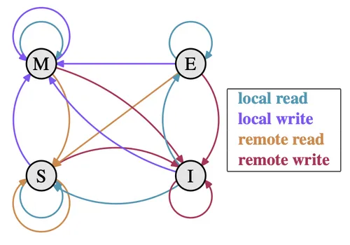
Image Credit: Based on a diagram from “What Every Programmer Should Know About Memory” by Ulrich Drepper.
The four MESI states are:
- M (Modified): The cache line is present only in the current cache and has been modified. The data in main memory is stale. This cache is responsible for writing the modified data back to main memory before any other cache can read it. A write can be performed on a Modified line without any bus transaction.4
- E (Exclusive): The cache line is present only in this cache, and its contents are consistent with main memory. Since this cache has the only copy, it can be written to locally without notifying other caches, at which point its state transitions to Modified. This is an optimization that avoids bus traffic for read-followed-by-write sequences.4
- S (Shared): The cache line may be present in this cache and in one or more other caches. Its contents are consistent with main memory. Data in a Shared line is effectively read-only. If a processor wishes to write to a Shared line, it must first issue an invalidation signal to other caches, after which it can claim exclusive ownership and transition its copy to the Modified state.4
- I (Invalid): The cache line does not contain valid data. This is the initial state of all cache lines and the state to which other lines transition when they are invalidated by another processor’s write.4
These state transitions ensure a coherent view of memory. For example, when a processor requests to read a memory location that is not in its cache (a read miss), it broadcasts a read request on the bus. If no other cache has the data, it is fetched from memory and placed in the requesting cache in the Exclusive state. If one or more other caches have the data in the Shared state, they respond, and the data is placed in the requesting cache in the Shared state. If another cache has the data in the Modified state, that cache intercepts the request, writes its modified data back to main memory, and then provides the data to the requesting cache, with both copies ending up in the Shared state.
The following table provides a simplified overview of state transitions that maintain coherence.
| Current State | Local Processor Read | Local Processor Write | Bus Read (Snoop) | Bus Write / Invalidate (Snoop) |
|---|---|---|---|---|
| Invalid (I) | Miss: Issue Bus Read. If other caches have it, go to Shared. If not, go to Exclusive. | Miss: Issue Read-For-Ownership (RFO). Go to Modified. | No action. | No action. |
| Shared (S) | Hit: No action. | Invalidate: Issue Bus Upgrade/RFO to invalidate other copies. Go to Modified. | No action (another cache has it). | Line is invalidated. Go to Invalid. |
| Exclusive (E) | Hit: No action. | Hit: No bus transaction needed. Go to Modified. | Another cache wants the data. Flush data to bus. Go to Shared. | Line is invalidated. Go to Invalid. |
| Modified (M) | Hit: No action. | Hit: No action. | Another cache wants the data. Flush data to bus (and write back to memory). Go to Shared. | Another cache is writing. Flush data to bus (and write back). Go to Invalid. |
References
Section titled “References”Footnotes
Section titled “Footnotes”-
Multi-core processor - Wikipedia, accessed October 2, 2025, https://en.wikipedia.org/wiki/Multi-core_processor ↩
-
Cache hierarchy - Wikipedia, accessed October 2, 2025, https://en.wikipedia.org/wiki/Cache_hierarchy ↩ ↩2 ↩3 ↩4
-
Cache Coherence | Redis, accessed October 2, 2025, https://redis.io/glossary/cache-coherence/ ↩ ↩2
-
Cache Coherency - Edward Bosworth, accessed October 2, 2025, http://www.edwardbosworth.com/My5155_Slides/Chapter13/CacheCoherency.htm ↩ ↩2 ↩3 ↩4 ↩5