4.1 Instruction-Level Parallelism (ILP)
Instruction-Level Parallelism (ILP) refers to the set of hardware-level techniques used to execute multiple instructions from a sequential program simultaneously within a single processor core. The primary objective of ILP is to increase the number of Instructions Per Cycle (IPC), thereby improving the performance of a single instruction stream. This section details the core techniques that enable ILP and examines the architectural limits of this paradigm through a case study of the Intel NetBurst™ microarchitecture.
4.1.1 Techniques for Instruction-Level Parallelism
Section titled “4.1.1 Techniques for Instruction-Level Parallelism”Modern processors employ a combination of techniques to discover and exploit ILP. These techniques work together to maximize the utilization of the processor’s multiple execution units.
Table 4.1: Core Techniques for Achieving Instruction-Level Parallelism
| Technique | Purpose |
|---|---|
| Pipelining | Overlaps the execution of multiple instructions by breaking each instruction’s processing into a series of discrete stages (e.g., Fetch, Decode, Execute, Write-Back).1 |
| Superscalar Execution | Executes multiple instructions per clock cycle by dispatching them to redundant functional units (e.g., multiple ALUs, FPUs).1 |
| Out-of-Order (OoO) Execution | Hides instruction dependencies and memory latency by allowing instructions to execute as soon as their operands are available, rather than in strict program order.2 |
| Speculative Execution & Branch Prediction | Mitigates control flow disruptions by predicting the outcome of conditional branches and executing instructions from the predicted path before the branch is resolved.1 |
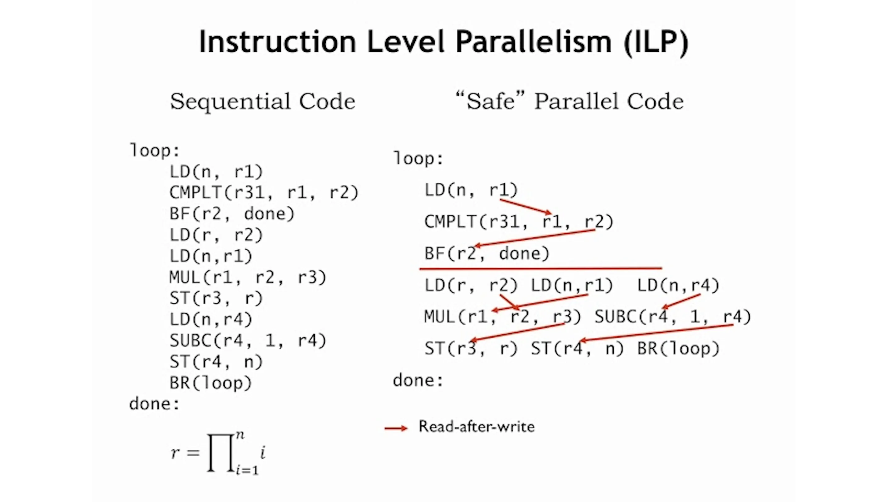
An example of Instruction-Level Parallelism, where independent instructions are reordered to execute in parallel, while respecting data dependencies. Credit: MIT OpenCourseWare.
Out-of-Order (OoO) execution is a key technique for hiding latency. It decouples instruction fetching from execution using a hardware scheduler that dispatches ready instructions to available execution units. A reorder buffer (ROB) ensures that the results are committed in the original program order to maintain correctness, allowing the processor to execute other instructions while long-latency operations are pending.2
4.1.2 Case Study: The NetBurst Microarchitecture and the Power Wall
Section titled “4.1.2 Case Study: The NetBurst Microarchitecture and the Power Wall”The Intel NetBurst™ microarchitecture, which powered the Pentium 4 processor, represents a case study in the limits of ILP and frequency scaling. Its design was based on the assumption that high clock frequencies could compensate for a lower IPC.
Architectural Characteristics
Section titled “Architectural Characteristics”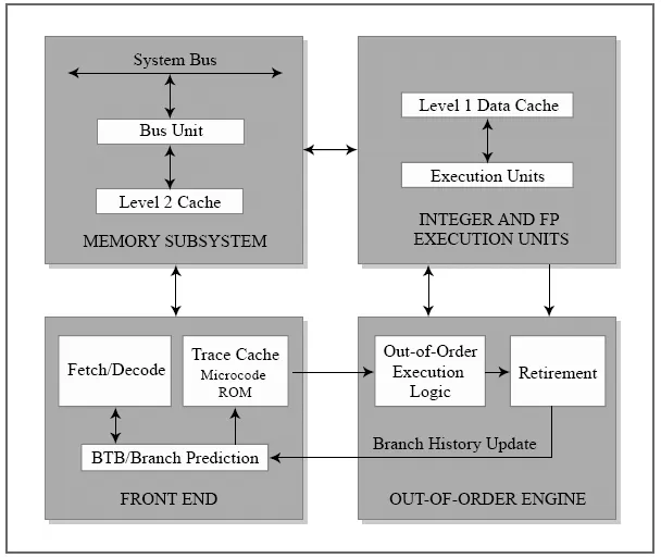
The block diagram of the Intel NetBurst microarchitecture. Credit: Fasiku, A., Olawale, J., & Jinadu, O. (2012). A Review of Architectures -Intel Single Core, Intel Dual Core and AMD Dual Core Processors and the Benefits. International Journal of Engineering and Technology, 2, 809-817.
The core design philosophy of NetBurst led to several key architectural decisions:
- Hyper-Pipelined Technology: To achieve high clock speeds, the instruction pipeline was made very deep. The initial “Willamette” core had a 20-stage pipeline, which was later extended to 31 stages in the “Prescott” core. This contrasts with the 10-stage pipeline of its P6 predecessor.3
- IPC/Frequency Trade-Off: The design explicitly traded a lower number of instructions per cycle for a much higher clock frequency. Intel projected that the architecture would scale to 10 GHz, where the high frequency would be the dominant factor in performance.3
- Advanced ILP Features: To compensate for the lower IPC, NetBurst included an advanced dynamic execution engine, an “Execution Trace Cache” to store decoded micro-operations, and a “Rapid Execution Engine” where simple integer ALUs ran at twice the core clock speed.4
Consequences and Collision with the Power Wall
Section titled “Consequences and Collision with the Power Wall”The pursuit of high frequency had several consequences:
- Branch Misprediction Penalty: The deep pipeline meant that an incorrect branch prediction incurred a significant penalty. Flushing and refilling 20-31 pipeline stages incurred a large cycle penalty, reducing the benefits of the high clock speed.4
- The Power Wall: A primary factor in NetBurst’s limitations was its power consumption. The combination of high frequencies and increasing transistor power leakage on the 90nm process node resulted in high power draw and heat generation. The Prescott core’s Thermal Design Power (TDP) reached 115 watts for a single core, a level that was difficult to manage with conventional cooling.3
The architecture that was designed to scale to 10 GHz encountered a physical limit at 3.8 GHz, not due to logic design constraints, but because of the inability to power and cool the chip effectively.
“With this microarchitecture, Intel planned to attain clock speeds of 10 GHz, but because of rising clock speeds, Intel faced increasing problems with keeping power dissipation within acceptable limits. Intel reached a speed barrier of 3.8 GHz in November 2004 but encountered problems trying to achieve even that… The reason for NetBurst’s abandonment was the severe heat problems caused by high clock speeds.” 3
Legacy
Section titled “Legacy”The limitations of the NetBurst microarchitecture were significant for the microprocessor industry. It demonstrated that performance scaling through frequency alone was no longer viable. This led to Intel’s shift to the “Core” microarchitecture, which abandoned the deep pipeline approach in favor of a wider, more power-efficient design that prioritized higher IPC at lower clock speeds. This event marked the industry-wide shift toward multi-core processors as the primary path forward for performance scaling.5
References
Section titled “References”Footnotes
Section titled “Footnotes”-
Instruction Level Parallelism (ILP), accessed October 2, 2025, https://eecs.ceas.uc.edu/~wilseypa/classes/eece7095/lectureNotes/ilp/ilp.pdf ↩ ↩2 ↩3
-
CPU Architecture: Instruction-Level Parallelism, accessed October 2, 2025, https://www.cs.cmu.edu/afs/cs/academic/class/15418-s21/www/lectures/02_ilp.pdf ↩ ↩2
-
NetBurst - Wikipedia, accessed October 2, 2025, https://en.wikipedia.org/wiki/NetBurst ↩ ↩2 ↩3 ↩4
-
The Microarchitecture of the Pentium 4 Processor - Washington, accessed October 2, 2025, https://courses.cs.washington.edu/courses/cse378/10au/lectures/Pentium4Arch.pdf ↩ ↩2
-
Multi-core processor - Wikipedia, accessed October 2, 2025, https://en.wikipedia.org/wiki/Multi-core_processor ↩