2.1 Limits of Single-Processor Performance
While Amdahl’s and Gustafson’s laws provide a theoretical framework for the performance of parallel systems, the industry’s widespread shift to parallelism was not merely an academic choice—it was an engineering necessity. This transition was forced by the unavoidable collision of single-processor architecture with three fundamental barriers. The end of single-core scaling was not a single event but a result of these multiple, systemic limitations, which are deeply interconnected. The pursuit of more Instruction-Level Parallelism led to more complex, power-hungry circuits, presenting designers with the Power Wall. The performance gains that were achieved only served to increase the gap between the processor and main memory, exacerbating the Memory Wall. The system was fundamentally imbalanced, and the prevailing paradigm for performance improvement ceased to be viable.1
2.1.1 The Power Wall
Section titled “2.1.1 The Power Wall”The most immediate of the three barriers was the Power Wall: the physical limit where a microprocessor becomes too hot to function. For years, the primary strategy for increasing performance was to raise the clock speed.2 This pursuit of higher clock frequencies was fueled by Moore’s Law, which allowed transistors to be shrunk and packed more densely. Denser packing meant shorter signal paths, enabling faster clock frequencies.3 However, this strategy had a significant thermodynamic cost. The power consumed by a CMOS transistor, the building block of modern CPUs, is governed by a crucial relationship: P = C × V² × F (where P is power, C is capacitance, V is voltage, and F is frequency). As architects increased frequency (F) and transistor density (which increases total capacitance, C), power consumption began to grow at an unsustainable, super-linear rate.3 A fundamental law of physics dictates that all electrical power consumed by a circuit is ultimately radiated as heat.2 Consequently, the power density of CPUs, measured in watts per square centimeter, increased to levels that could not be managed by inexpensive air-cooling solutions.2 Case Study: The NetBurst Architecture Intel’s “NetBurst” architecture, which powered the Pentium 4, is a prominent example of the limitations imposed by the Power Wall. It was explicitly designed with the goal of scaling to 10 GHz. However, the architecture was affected by significant thermal issues. The “Prescott” revision, for example, idled at 50°C (122°F) and dissipated around 100 watts under load.4 The thermal management problems became so significant that Intel was forced to abandon the entire architecture, canceling its 4 GHz single-core developments and changing the company’s product roadmap.5 This encounter with the Power Wall is visible in the industry’s own projections. Roadmaps from the early 2000s predicted clock speeds in the 12–15 GHz range by 2015. These forecasts were quickly revised as the practical and economic limits of cooling were reached.2 The rate of single-core performance improvement, which had averaged 52% per year from 1986 to 2002, decreased to approximately 6% per year afterward.
| Era | Annual Performance Growth | Primary Driver |
|---|---|---|
| 1986–2002 | ~52% | Clock Frequency Scaling |
| Post-2002 | ~6% | Architectural Tweaks |
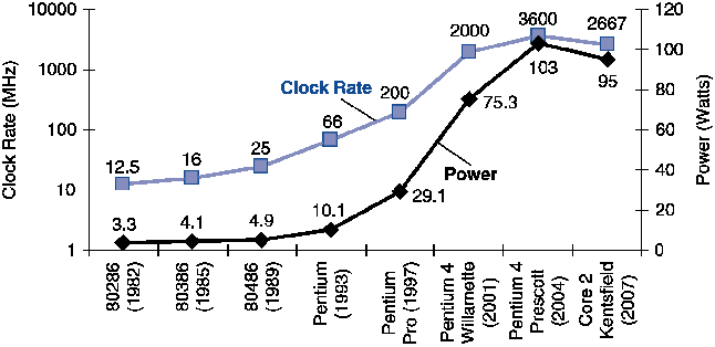
Clock rate and power consumption trends showing the power wall crisis. As clock rates approached their physical limits, power consumption continued to rise unsustainably. Image Credit: Patterson & Hennessy
The industry shifted to a new direction. While high-end, cost-insensitive sectors like mainframes could resort to specialized solutions—such as the sophisticated water-cooling systems used by IBM to run its POWER6 CPUs at over 5.0 GHz—this was not a viable path for the mass market.6 For commodity providers like Intel and AMD, the only logical and economically feasible solution was to abandon the frequency race. They began using the ever-increasing transistor budget from Moore’s Law not to make one core faster, but to place multiple, simpler, more power-efficient cores onto a single chip.2 This led to the development of multi-core processors, marking the beginning of the multi-core era.
2.1.2 The Memory Wall
Section titled “2.1.2 The Memory Wall”Running parallel to the thermal crisis was the Memory Wall, a second significant barrier representing the growing performance gap between processors and main memory. As discussed in the foundational principles, this disparity forced increasingly powerful processors to spend a substantial fraction of their time idle, awaiting data from comparatively slow DRAM.7
A single main memory access can incur a modern processor 200 to 300 CPU cycles—a significant period of processor inactivity during which no useful work is performed.8 To mitigate this, architects implemented deep hierarchies of cache memories to exploit the principle of locality. However, caches serve as a mitigation strategy, not a complete solution. They defer, but do not eliminate, the costly retrieval from main memory. As processors became exponentially faster, the penalty for each “cache miss,” measured in lost cycles, grew exponentially as well.
This problem became particularly acute for data-intensive workloads, such as AI and big data analytics, which frequently operate on datasets too large to reside entirely within on-chip caches.9 For these applications, performance is often limited not by computation but by memory bandwidth—the rate at which data can be transferred. The Memory Wall, initially characterized primarily by latency, has evolved to encompass both latency and bandwidth limitations, remaining a persistent challenge among the three walls.10
2.1.3 The Instruction-Level Parallelism (ILP) Wall
Section titled “2.1.3 The Instruction-Level Parallelism (ILP) Wall”The third barrier, the Instruction-Level Parallelism (ILP) Wall, is an architectural one, representing the point of diminishing returns in the effort to extract more parallelism from a single, sequential instruction stream.11 For much of the 1990s, exploiting ILP was the primary engine of performance growth beyond raw clock speed. Architects developed a sophisticated set of techniques to allow a processor to execute multiple instructions simultaneously, creating what one author called the “serial illusion” for the programmer.12 Techniques for Instruction-Level Parallelism
- Pipelining: This fundamental technique overlaps the execution stages of multiple instructions. A five-stage pipeline can be working on five different instructions at once, but its efficiency is limited by “hazards,” where one instruction depends on the result of a preceding one, forcing a stall.2
- Superscalar Execution: This involves building processors with multiple parallel functional units (e.g., multiple adders, multipliers) that can issue and execute several independent instructions in the same clock cycle.13
- Out-of-Order Execution: This allows the processor to dynamically reorder the instruction stream at runtime, searching ahead for independent instructions it can execute while a stalled instruction is waiting for its dependencies to be resolved.
- Speculative Execution & Branch Prediction: To keep the pipeline full in the presence of conditional branches (if-then statements), the processor guesses the outcome and begins executing instructions from the predicted path. If the prediction is correct, performance is gained; if it is wrong, the speculative results are flushed, incurring a significant performance penalty and wasting the energy spent on the incorrect path.1
These techniques were highly successful, accounting for up to a seven-fold speedup over simple execution.14 However, this gain came at a substantial and ultimately unsustainable cost in complexity and power consumption. Each successive improvement in ILP required a super-linear increase in chip complexity, transistor count, and power consumption for what was often a sub-linear improvement in real-world performance.15 The effort to extract finer grains of parallelism was described as “digging a deeper power hole,” directly linking the ILP Wall to the Power Wall.16 Ultimately, the pursuit of ILP ran into a more fundamental limit: the amount of parallelism inherent in typical programs. Seminal studies on the limits of ILP, such as those by David W. Wall, simulated idealized processors with features such as perfect branch prediction and perfect memory analysis.17 Even under these perfect conditions, the analysis showed that the average parallelism available in common integer benchmark programs rarely exceeds 7, with a more typical value being around 5.17 This indicated that the investment in hardware complexity was targeting a limited resource. The ILP Wall, therefore, represents the point where the cost-benefit trade-off for extracting more ILP became unfavorable, forcing architects to seek performance from other, more explicit sources of parallelism.
References
Section titled “References”Footnotes
Section titled “Footnotes”-
370 lecture #23 — Fall 2002, accessed October 1, 2025, https://web2.qatar.cmu.edu/~msakr/15447-f08/lectures/Lecture27.ppt ↩ ↩2
-
The Power Wall For CPU Chips - Edward Bosworth, accessed October 1, 2025, http://www.edwardbosworth.com/My5155_Slides/Chapter01/ThePowerWall.htm ↩ ↩2 ↩3 ↩4 ↩5 ↩6
-
Chapter 2 – The Power Wall and Multicore Computers - Edward Bosworth, accessed October 1, 2025, http://www.edwardbosworth.com/My5155Text_V07_PDF/MyText5155_Ch02_V07.pdf ↩ ↩2
-
Pentium 4 - Wikipedia, accessed October 1, 2025, https://en.wikipedia.org/wiki/Pentium_4 ↩
-
Computer Architecture: A Quantitative Approach, accessed October 1, 2025, https://acs.pub.ro/~cpop/SMPA/Computer%20Architecture%20A%20Quantitative%20Approach%20(5th%20edition).pdf ↩
-
The Power Wall - Edward Bosworth, accessed October 1, 2025, http://www.edwardbosworth.com/My5155_Slides/Chapter01/ThePowerWall.pdf ↩
-
Say Goodbye to the Memory Wall - UVA Today - The University of Virginia, accessed October 1, 2025, https://news.virginia.edu/content/say-goodbye-memory-wall ↩
-
Untitled - CERN Indico, accessed October 1, 2025, https://indico.cern.ch/event/59397/contributions/2050044/attachments/996317/1416877/SS_lazzaro.pdf ↩
-
What is the “Memory-Wall” in Modern Computing and AI custom …, accessed October 1, 2025, https://medium.com/@anan.mirji/what-is-the-memory-wall-in-modern-computing-and-ai-custom-silicon-b2b33fcd08f3 ↩
-
What is the memory wall in computing? - Ayar Labs, accessed October 1, 2025, https://ayarlabs.com/glossary/memory-wall/ ↩
-
CLOSED Call for Papers: Special Section on Parallel and Distributed Computing Techniques for Non-Von Neumann Technologies, accessed October 1, 2025, https://www.computer.org/digital-library/journals/td/call-for-papers-special-section-on-parallel-and-distributed-computing-techniques-for-non-von-neumann-technologies/ ↩
-
Optional Prereading - aiichironakano, accessed October 1, 2025, https://aiichironakano.github.io/cs596/Prereading-Reinders-Marusarz-August-4.pdf ↩
-
Instruction-level parallelism - Wikipedia, accessed October 1, 2025, https://en.wikipedia.org/wiki/Instruction-level_parallelism ↩
-
Computer Architecture and the Wall - SemiWiki, accessed October 1, 2025, https://semiwiki.com/general/1047-computer-architecture-and-the-wall/ ↩
-
(PDF) A Survey on Parallel Architectures and Programming Models, accessed October 1, 2025, https://www.researchgate.net/publication/344832796_A_Survey_on_Parallel_Architectures_and_Programming_Models ↩
-
Solved “Power Wall + Memory Wall + ILP Wall = Brick | Chegg.com, accessed October 1, 2025, https://www.chegg.com/homework-help/questions-and-answers/power-wall-memory-wall-ilp-wall-brick-wall-components-brick-wall-1-power-wall-means-faster-q722182223 ↩
-
Limits of Instruction-Level Parallelism, accessed October 1, 2025, https://www.eecs.harvard.edu/cs146-246/wall-ilp.pdf ↩ ↩2